Nano and Giga Challenges in Electronics, Photonics and Renewable Energy
Current Trends in Radiophysics
Symposium and Summer School (Tutorial Lectures)
Tomsk, Russia, September 18-22, 2017
nanoandgiga.com/ngc2017 and apr.tsu.ru
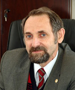
Commentary Grigory Dunaevsky
To read Dunaevsky's commentary in Russian published in STRF.RU click here
Representatives of the world research community will gather at Tomsk State University to discuss ongoing research and developments, trends and changes in electronic and semiconductor industry.
The first trend is changes in the production technology of new semiconductor materials based on complex multicomponent compounds of germanium, silicon, indium, and gallium, which are nowadays replacing substrates of silicon, gallium arsenide and other traditional materials. Specialists of TSU are members of scientific consortia that work on the development of technologies and equipment for manufacturing complex multicomponent semiconductor wafers and defect-free crystals. These materials are being tested today in manufacturing products for radio electronics, alternative energy, and portable power sources. Problems of process development to produce such materials are relevant for material scientists all around the world and for those who will participate in the International Forum NGC / CTRP 2017.
The second trend in electronics today is the creation of technologies to obtain a low-dimensional element base and to solve issues related to the creation of devices with reduced power consumption and voltage, high-density charge and energy storage, as well as the development of microcircuits for work in extreme conditions (Space, the Arctic), intelligent networks of sensors, and micro-robots. At the same time, the technology of semiconductor materials and microcircuits is significantly changing as a result of the reduction in size of planar and two-dimensional elements and the increasing complexity of the formation of nanoscale structures for the manufacturing of products with a minimum element size of 20 nm. The need for integration-heterointegration technology (it increases the compactness of the placement of devices when using planar technology) and 3D integration, is growing. It provides a high density of integration of small components on small devices by compact placement of elements not only in the plane but also in the volume of material (layered formation of elements of the devices).
The third trend that is extremely promising is associated with the use of organic materials in electronics. These works are also conducted at TSU. A section devoted to this topic is planned to be held at the Forum.When working with integration technologies and switching to nanotechnology, the design of materials and products plays a huge role. A number of reports and discussions between local and invited experts at the Forum will be devoted to this topic. There will be an event for students of Russian universities held by the representatives of the leading companies of the Silicon Valley on programming on chips and computer architecture.
Our Sponsors and Partners