PROGRAM
REGISTRATION
LOCAL
ARCHIVE
|
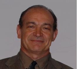
Commentary Gennadi Bersuker
Nano & Giga Forum Meets Challenges
|

|
Charge transfer in thin oxide stacks (which are employed, for instance, in highly scaled electron devices, energy storage structures, etc.) can be strongly affected by a tiny amount of atomic defects (< 1E-17/cm3), detection of which might be way beyond the sensitivity of the most physical characterization methods. This circumstance leaves the electrical sensing techniques to be a preferred and, in some cases, the only option. Extracting defect information from electrical data, however, presents a challenging task of connecting the physical processes associated with the specific electrical measurement to the defect atomic structure. The measurements of interest are based on the processes of the charged carrier tunneling to (from) and capture (emission) at the defect site. The characteristic times of these events is usually dominated by the capture/emission processes and, hence, determined by the structural and electronic properties of the defect and surrounding lattice. Therefore, these characteristic times present a signature of the defect structure, and by comparing the measured and calculated (using the defect parameters obtained by ab initio calculations) times we can identify the nature of electrically-active defects. This general scheme was implemented in the software package simulating a variety of electrical measurements, each of which probe a specific range of energy and spatial defect distributions. Combining simulation results for a variety of the applied measurement techniques we obtain a complete picture of defect characteristics.
On a different note, I would like to comment on the NGC conferences. Technological needs evolve very fast these days forcing researchers to move along. And the well-managed conferences stay ahead of the trend rather than try catching up with it. Participating in NGC from its inception, I am amazed to see how much it has changed. A number of huge, cutting-edge companies (e.g., Motorola, which provided the initial kick-off support to this meeting) couldnÕt manage this change and disappeared from the technology race but NGC is alive and doing better than ever increasing its scope and attracting more people. I believe that this success reflects on the foresight of the conference organizers clustering in ASU, an institution, which does not afraid to give a chance to unconventional approaches. I really hope that NGC will continue evolving and remain the scientific gathering of choice, which unites researchers from a variety of areas.
|


